
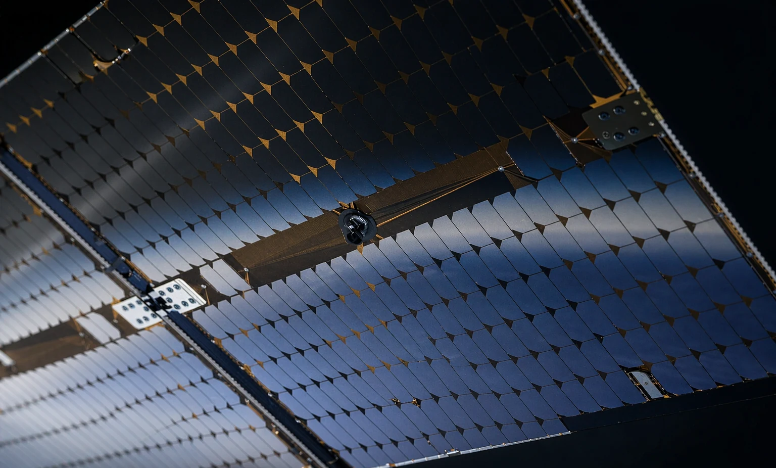
Fragmented supply
Epitaxy, chip processing and CIC assembly usually come from three different suppliers. Every interface is a separate qualification and a separate schedule risk.
Wafertop grows, processes and assembles triple-junction GaAs solar cells — 30 to 32% BOL efficiency, qualified to GJB 7392-2011, built at up to a million epitaxial wafers a year.
Four things determine whether a photovoltaic programme holds its schedule and its power budget. None of them is a cell-level specification — they are supply-chain properties.
Epitaxy, chip processing and CIC assembly usually come from three different suppliers. Every interface is a separate qualification and a separate schedule risk.
Efficiency spread across lots does not stay at cell level — it becomes array-level power loss, discovered late at panel integration.
End-of-life power sizes the array, not beginning-of-life. Without published 1 MeV degradation data, that margin is guesswork.
A constellation needs tens of thousands of cells on a repeatable schedule. Qualification lots are not a capacity plan.
Six numbers that describe the plant behind the datasheet.
Lattice-matched AlGaInP/InGaAs/Ge triple junction, in mass production — not a laboratory result.
30 – 32% BOL800,000 to 1,000,000 four-inch-equivalent wafers a year across thirteen Aixtron MOCVD 2800 G4 reactors, supplemented by leased tools.
1,000,000 wafersA complete in-house solar-cell line — 200,000 to 240,000 chips a year: lithography, etching, coating, thinning, dicing and test.
240,000 chipsGe substrates in 4-inch and 6-inch, with 6 µm epitaxial layers and EPD below 300/cm².
4" & 6"Founding team with programmes for the Chinese Space Station, lunar rovers and satellite power systems.
25+ yearsEvery space cell type in this catalogue is fully qualified to the national space standard.
GJB 7392-2011We are the single supplier for the three steps that usually take three vendors — which is the answer to problem 01 above.
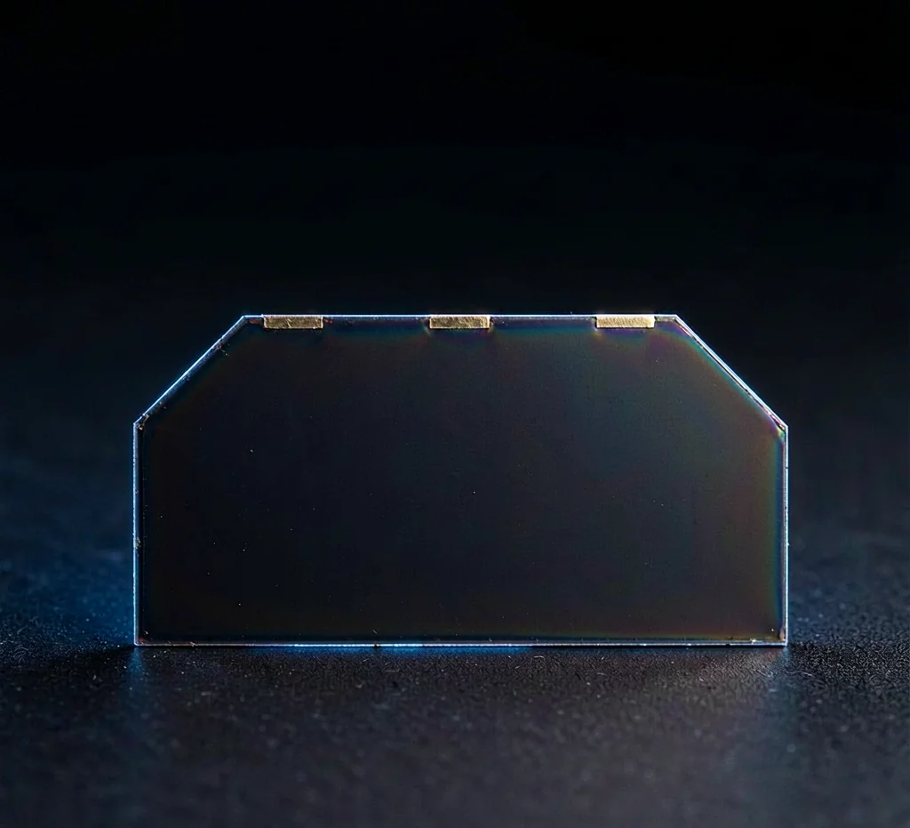
Lattice-matched AlGaInP/InGaAs/Ge on Ge, delivered bare or as a finished CIC — 4080 or 14468 — with coverglass, interconnectors and bypass diode.
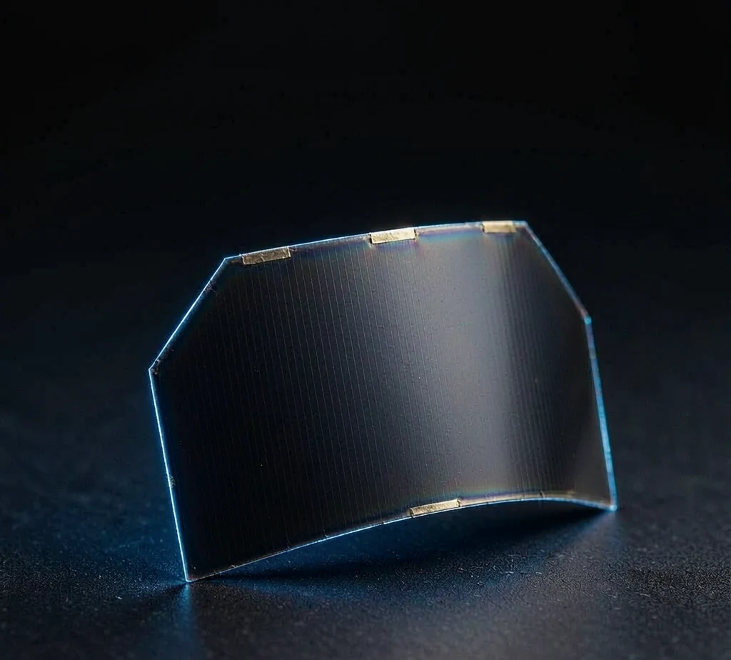
AlGaInP/GaAs/InGaAs lifted off the growth wafer — 31.5% on polyimide, 30.5% on metal substrate — for platforms where specific power sets the mission.
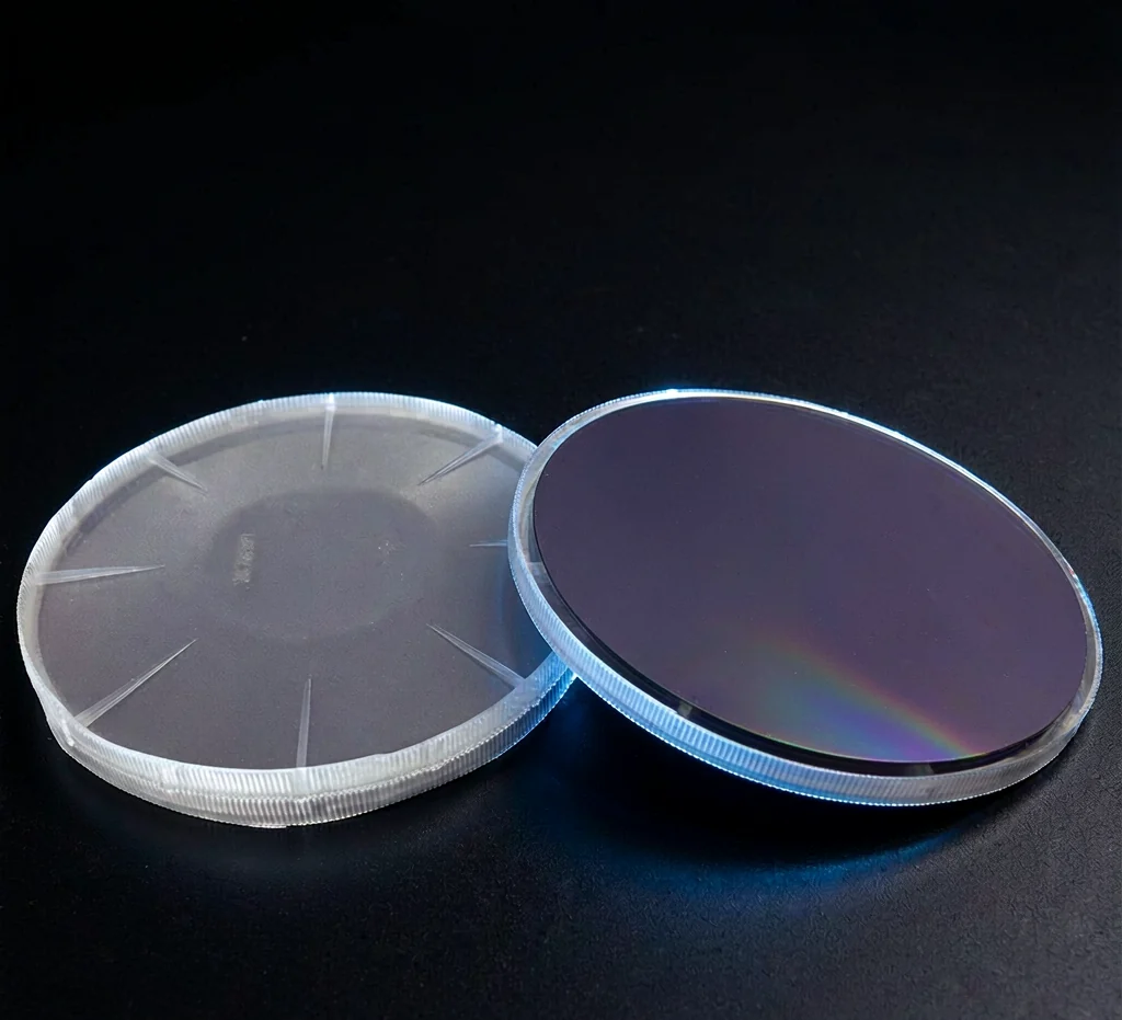
4-inch and 6-inch Ge-based wafers for customers running their own cell process, or needing a custom design on a qualified stack.
Assembly components — coated coverglass (Tave ≥ 93.5%), Si bypass diodes and space-grade interconnectors — are supplied with the cell or separately. See components →
Product imagery is derived from photographs of our own hardware and restaged for presentation. Minor visual detail may differ from delivered parts — the tabulated dimensions and electrical data are the binding reference.
Three properties decide what a cell delivers at end of life — not what it measures on the flash tester at beginning of life.
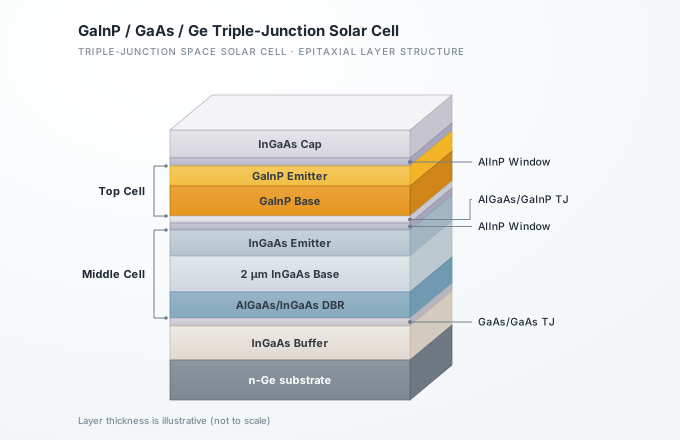
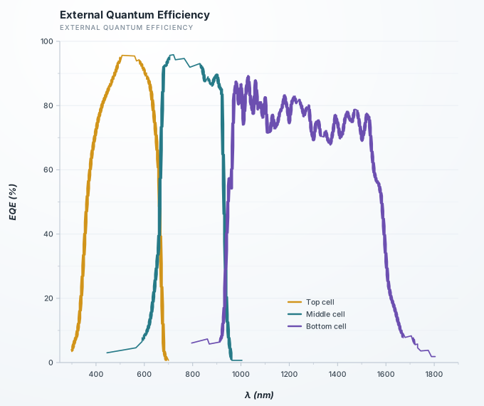
GaInP / GaAs / Ge sub-cells joined by tunnel junctions, each absorbing a different band of the spectrum — grown in-house on our own MOCVD reactors.
1 MeV electron degradation and temperature coefficients are part of the datasheet, so end-of-life power can be calculated rather than assumed.
Flexible cells at 30 µm and 28 mg/cm² — the same epitaxy, released from the growth substrate onto metal foil.
From GEO telecom platforms to CubeSat deployables and high-altitude aircraft — the same epitaxy, tuned to the radiation and mass budget of each mission.
Repeatable batch performance and volume pricing for large flat-panel arrays.
Radiation-hard triple-junction cells for 15-year GEO missions and deep-space probes.
30 µm flexible cells at 28 mg/cm² for deployable and body-mounted arrays.
Lightweight thin-film cells for high-altitude pseudo-satellites and long-endurance aircraft.
Founded in 2021 and headquartered in Xiamen, Wafertop is a national high-tech enterprise focused on III–V compound semiconductor epitaxy, chip R&D and industrialisation. We hold ISO 9001 certification, and our cells are exported to customers across multiple countries and regions.
Beyond photovoltaics, the same MOCVD platform produces 940 nm VCSEL epitaxial wafers, edge-emitting lasers and InGaAs PIN/APD detector wafers.
Cell size, orbit, radiation dose and annual quantity — we will come back with a specification and a price.
Request a quote