
Space solar cells,
assemblies and epi wafers
Every figure below is taken from the current published datasheet. Electrical data is measured at AM0, 1 sun, 1353 W/m², 25 °C unless stated otherwise.
Triple-junction GaAs solar cell assemblies
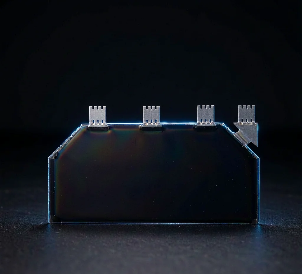
AlGaInP/InGaAs/Ge on Ge substrate, supplied as a finished CIC with external silicon bypass diode, interconnectors and coverglass. One stack, one qualification, offered in a 32% grade and a 30% grade, in 80 × 40 mm and 144 × 68 mm formats.
| Parameter | 4080CIC- N32TBLBAP |
4080CIC- N30TBLBA |
14468CIC- N30TBLBA |
|---|---|---|---|
| Efficiency class | 32% | 30% | 30% |
| Average η (%) | 32 | 30.5 | 30.5 |
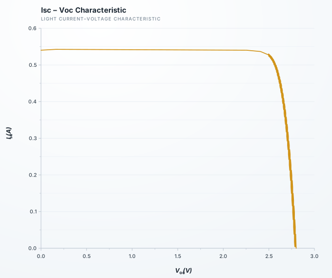
| Voc (mV) | 2775 | 2750 | 2750 |
| Jsc (mA/cm²) | 18 | 17.6 | 17.6 |
| Vm (mV) | 2450 | 2430 | 2430 |
| Jm (mA/cm²) | 17.5 | 17 | 17 |
| Dimensions (mm) | 80.15 × 40.15 | 80.15 × 40.15 | 144.45 × 68.65 |
| Cell area (cm²) | 30.15 | 30.15 | 79.8 |
| Weight (mg/cm²) | 120 ± 15 | 120 ± 15 | 165 ± 15 |
| Thickness (µm) | 360 ± 30 | 360 ± 30 | 440 ± 30 |
| ILavg @ 2300 mV (mA) | 515 | 500 | 1345 |
| Pm/Pm0 @ 1E15 | 0.86 | 0.855 | 0.855 |
The two 4080 grades are mechanically identical — same footprint, same 30.15 cm² area, same 120 mg/cm² mass — so a programme can change efficiency grade without re-qualifying its array interface. One 14468 covers 2.6× the area of one 4080 at the same current density, which cuts the cell, interconnect and weld count per square metre by roughly 62%.
- Fully qualified according to GJB 7392-2011
- 32% BOL efficiency in batch production
- Custom sizes available
| Base material | AlGaInP/InGaAs/Ge on Ge substrate |
|---|---|
| AR coating | TiOx/Al2O3 |
| Dimensions | (80.15 ± 0.1) × (40.15 ± 0.1) mm |
| Cell area | 30.15 cm² |
| Weight | 120 ± 15 mg/cm² |
| Thickness (without contacts) | 360 ± 30 µm |
| Coverglass thickness | 120 ± 20 µm |
| Interconnectors | Kovar, silver coated |
| Interconnector thickness | 25 µm |
| Bypass protection | External Si diode |
| Average open-circuit voltage Voc | 2775 mV |
|---|---|
| Average short-circuit current Jsc | 18 mA/cm² |
| Average voltage at max. power Vm | 2450 mV |
| Average current at max. power Jm | 17.5 mA/cm² |
| Average efficiency η | 32 % |
| Parameter | 1E14 | 3E14 | 1E15 |
|---|---|---|---|
| Im/Im0 | 0.99 | 0.98 | 0.94 |
| Vm/Vm0 | 0.94 | 0.92 | 0.91 |
| Pm/Pm0 | 0.94 | 0.91 | 0.86 |
| Voltage VL | 2300 mV |
|---|---|
| Min. average current ILavg @ VL | 515 mA |
| Min. individual current ILmin @ VL | 495 mA |
| Parameter | BOL | 1E15 |
|---|---|---|
| Jsc (µA/cm²/°C) | 10.0 | 12.7 |
| Voc (mV/°C) | −6.1 | −6.5 |
| Jm (µA/cm²/°C) | 9.2 | 15.2 |
| Vm (mV/°C) | −6.2 | −6.8 |
| Absorptivity | ≤ 0.92 |
|---|---|
| Pull test (at 45°) | ≥ 0.83 N/mm² |
| Status | Qualified |
- Fully qualified according to GJB 7392-2011
- 30% BOL efficiency in batch production
- Same assembly BOM as the 32% grade — coverglass, Kovar interconnectors, external Si diode
| Parameter | 4080 | 14468 |
|---|---|---|
| Dimensions (mm) | 80.15 × 40.15 | 144.45 × 68.65 |
| Cell area (cm²) | 30.15 | 79.8 |
| Weight (mg/cm²) | 120 ± 15 | 165 ± 15 |
| Thickness (mm) | 0.360 ± 0.030 | 0.440 ± 0.030 |
| Voltage VL (mV) | 2300 | 2300 |
| ILavg @ VL (mA) | 500 | 1345 |
| ILmin @ VL (mA) | 480 | 1333 |
| Base material | AlGaInP/InGaAs/Ge on Ge substrate |
|---|---|
| AR coating | TiOx/Al2O3 |
| Coverglass thickness | 120 ± 20 µm |
| Interconnectors | Kovar, silver coated, 25 µm |
| Bypass protection | External Si diode |
| Parameter | 1E14 | 3E14 | 1E15 |
|---|---|---|---|
| Im/Im0 | 0.99 | 0.98 | 0.94 |
| Vm/Vm0 | 0.94 | 0.93 | 0.91 |
| Pm/Pm0 | 0.93 | 0.91 | 0.855 |
| Parameter | 4080 | 14468 |
|---|---|---|
| Jsc, BOL (µA/cm²/°C) | 9.9 | 11.1 |
| Jsc, 1E15 | 12.8 | 13.1 |
| Voc, BOL (mV/°C) | −6.0 | −6.0 |
| Voc, 1E15 | −6.4 | −6.7 |
| Jm, BOL (µA/cm²/°C) | 9.1 | 9.1 |
| Jm, 1E15 | 15.1 | 15.1 |
| Vm, BOL (mV/°C) | −6.1 | −6.2 |
| Vm, 1E15 | −6.6 | −6.6 |
| Absorptivity | ≤ 0.92 |
|---|---|
| Pull test (at 45°) | ≥ 0.83 N/mm² |
| Status | Qualified |
Radiation data above applies to both 30% formats. Datasheets state the efficiency class as 30% while the electrical table lists 30.5% average η for batch production — we quote both rather than reconcile them. Full PDFs on request.
Triple-junction GaAs solar cell
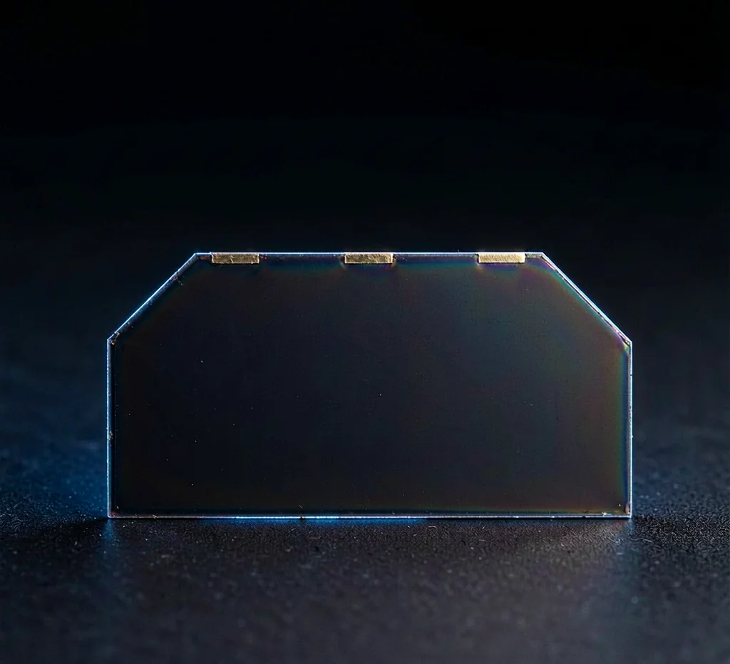
Large-area GaInP/InGaAs/Ge cell on Ge substrate for high-power rigid arrays, supplied as a bare cell with a three-pad grid.
- Fully qualified according to GJB 7392-2011
- 31% BOL efficiency in batch production
- Custom sizes available
| Base material | GaInP/InGaAs/Ge on Ge substrate |
|---|---|
| AR coating | TiOx/Al2O3 |
| Dimensions | (144.6 ± 0.1) × (66.5 ± 0.1) mm |
| Cell area | 77.26 cm² |
| Weight | 80 ± 10 mg/cm² |
| Thickness (without contacts) | 0.155 ± 0.025 mm |
| Contact metallisation (Ag/Au) | 4 – 7 µm |
| Grid design | Grid system with 3 contact pads |
| Average open-circuit voltage Voc | 2780 mV |
|---|---|
| Average short-circuit current Jsc | 17.8 mA/cm² |
| Average voltage at max. power Vm | 2450 mV |
| Average current at max. power Jm | 17.2 mA/cm² |
| Average efficiency η | 31 % |
| Parameter | 1E14 | 3E14 | 1E15 |
|---|---|---|---|
| Im/Im0 | 0.99 | 0.98 | 0.94 |
| Vm/Vm0 | 0.94 | 0.93 | 0.91 |
| Pm/Pm0 | 0.93 | 0.91 | 0.855 |
| Voltage VL | 2300 mV |
|---|---|
| Min. average current ILavg @ VL | 1345 mA |
| Min. individual current ILmin @ VL | 1333 mA |
| Parameter | BOL | 1E15 |
|---|---|---|
| Jsc (µA/cm²/°C) | 11.1 | 13.1 |
| Voc (mV/°C) | −6.0 | −6.7 |
| Jm (µA/cm²/°C) | 9.1 | 15.1 |
| Vm (mV/°C) | −6.2 | −6.6 |
| Absorptivity | ≤ 0.92 |
|---|---|
| Pull test (at 45°) | ≥ 0.83 N/mm² |
| Status | Qualified |
This is the bare cell — no coverglass, no interconnectors — for customers who assemble their own CIC. The 14468CIC-N30TBLBA above is a comparable large-area cell supplied as a finished assembly. Datasheet efficiency class 30%; 31% average BOL efficiency is stated for batch production in the current datasheet (2025.12). Contact us for the full PDF.
Triple-junction flexible GaAs solar cell
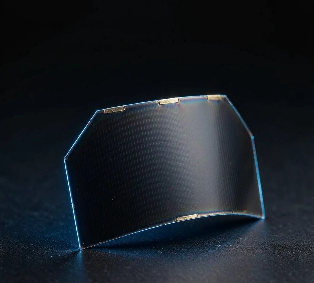
AlGaInP/GaAs/InGaAs lifted off the growth wafer. The 31.5% build sits on a 75 µm polyimide carrier; the 30.5% build on a 30 µm metal substrate. Both share the 80 × 40 mm footprint and the same eight-pad grid, so the choice between them is electrical, not mechanical.
| Parameter | RPM31T030AB 31.5% class |
Metal substrate 30.5% class |
|---|---|---|
| Efficiency class | 31.5% | 30.5% |
| Average η (%) | 31.8 | 30.5 |
| Voc (mV) | 3000 | 3050 |
| Jsc (mA/cm²) | 16.8 | 16.2 |
| Vm (mV) | 2655 | 2700 |
| Jm (mA/cm²) | 16.2 | 15.6 |
| Substrate | Polyimide (PI) | Metal |
| Dimensions (mm) | 80.0 × 40.0 | 80.0 × 40.0 |
| Cell area (cm²) | 30.15 | 29.4 |
| Thickness (mm) | 0.075 ± 0.02 | 0.030 ± 0.01 |
| Weight (mg/cm²) | 20 ± 5 | 28 ± 5 |
| Contact metallisation | Ag/Au, 4 – 7 µm | Ag/Au, 4 – 7 µm |
| Pm/Pm0 @ 1E15 | 0.825 | 0.85 |
The 31.5% build trades radiation hardness for beginning-of-life power: at 1E15 e/cm² it retains 82.5% of its power against 85% for the metal build, but starts 1.3 points higher. On a low-fluence mission the PI build wins outright; in a harsh orbit the metal build closes the gap.
- Fully qualified according to GJB 7392-2011
- Flexible, lightweight, custom sizes available
- Eight-pad grid on both builds; Ag/Au contacts 4 – 7 µm
| Parameter | 31.5% · PI | 30.5% · metal |
|---|---|---|
| Im/Im0 @ 1E14 | 0.99 | 0.98 |
| Im/Im0 @ 3E14 | 0.96 | 0.97 |
| Im/Im0 @ 1E15 | 0.93 | 0.93 |
| Vm/Vm0 @ 1E14 | 0.94 | 0.94 |
| Vm/Vm0 @ 3E14 | 0.92 | 0.93 |
| Vm/Vm0 @ 1E15 | 0.89 | 0.91 |
| Pm/Pm0 @ 1E14 | 0.94 | 0.92 |
| Pm/Pm0 @ 3E14 | 0.88 | 0.90 |
| Pm/Pm0 @ 1E15 | 0.825 | 0.85 |
| Parameter | BOL | 1E15 |
|---|---|---|
| Jsc (µA/cm²/°C) | 9.5 | 13.7 |
| Voc (mV/°C) | −6.22 | −6.8 |
| Jm (µA/cm²/°C) | 9.0 | 13.0 |
| Vm (mV/°C) | −6.2 | −7.1 |
| Absorptivity | ≤ 0.92 |
|---|---|
| Pull test (at 45°) | ≥ 0.83 N/mm² |
| Status | Qualified |
| Datasheet efficiency class | 31.5% stated, 31.8% in the electrical table |
|---|---|
| 30.5% build substrate | Metal; datasheet gives 28 ± 5 mg/cm² at 0.030 mm |
Triple-junction solar cell epitaxial wafers
Ge-based epi wafers in 4-inch and 6-inch, for customers who run their own cell processing or need a custom cell design on a standard stack.
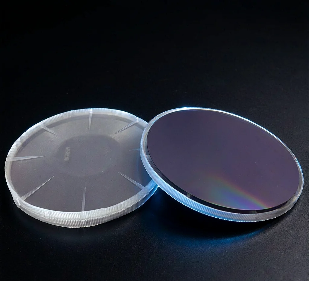
- 30.8% BOL efficiency at wafer level in batch production
- Suitable for any further processing and custom cell designs
- 4-inch and 6-inch epitaxial wafers available
| Substrate type | Ge |
|---|---|
| Substrate thickness — 4" | 140 ± 10 µm |
| Substrate thickness — 6" | 225 ± 15 µm |
| Epitaxial layer thickness | 6 µm |
| Substrate size — 4" | 100.0 ± 0.25 mm |
| Substrate size — 6" | 150.0 ± 0.25 mm |
| Etch pit density (EPD) | < 300 /cm² |
| Parameter | BOL | 1E14 | 3E14 | 1E15 |
|---|---|---|---|---|
| Voc (mV) | 2750 | 2596 | 2540 | 2497 |
| Jsc (mA/cm²) | 17.6 | 17.5 | 17.2 | 16.9 |
| Fill factor FF (%) | 86.0 | 85.8 | 85.2 | 84.5 |
| Conversion efficiency (%) | 30.8 | 28.9 | 27.5 | 26.4 |
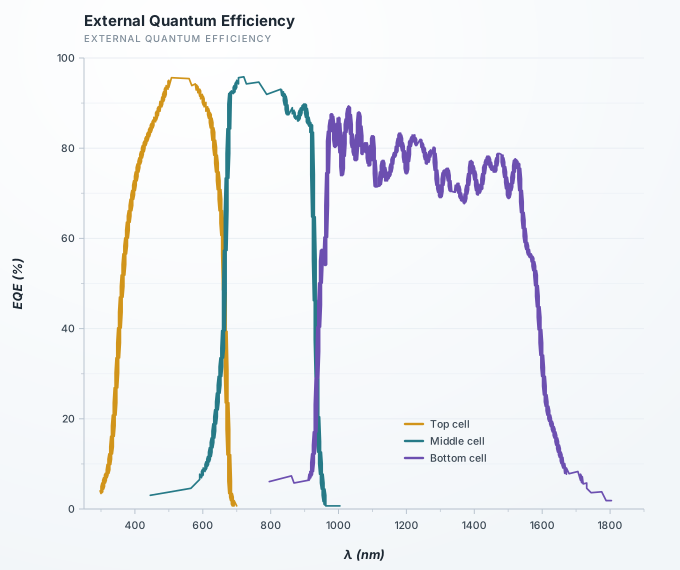
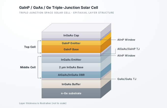
Coverglass, bypass diodes and interconnectors
Supplied together with our cells, or separately for customers assembling their own CICs.
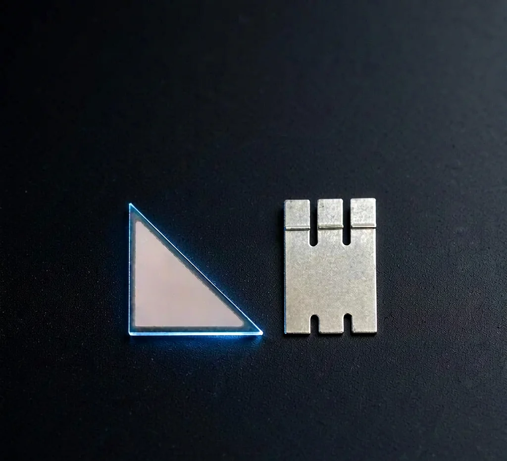
| Dimensions | 40.15 × 80.15 × 0.12 mm |
|---|---|
| Tave 400–1100 nm | ≥ 93.5% |
| Transmittance @ 400 nm | ≥ 90.5% |
| Transmittance @ 700 nm | ≥ 94% |
| Transmittance @ 1100 nm | ≥ 93.5% |
| Environmental | RoHS and halogen-free |
| Coating adhesion | 15 min boil + 3× CT-18 tape pull, no peel |
| Dot defects | ≤ 40 µm, max. 10 pcs, spacing ≥ 100 µm |
|---|---|
| Scratches | Not allowed |
| Edge chipping | Radial width ≤ 0.1 mm, no cracking |
| Cleanliness | Removable dust < 3%, no stains or fingerprints |
| Coating colour | Consistent, unchanged after cleaning |
| Bypass protection | External Si diode, one per CIC |
|---|---|
| Interconnector material | Kovar, silver coated |
| Interconnector thickness | 25 µm |
| Pull test (at 45°) | ≥ 0.83 N/mm² |
Coverglass dimension and coating figures are from our internal specification sheet; the space interconnector and bypass diode lines are supplied as part of every CIC assembly — 4080 and 14468, both grades. Contact us for component-level datasheets.
Product imagery is derived from photographs of our own hardware and restaged for presentation. Minor visual detail may differ from delivered parts — the tables are the binding reference for dimensions, electrical performance and qualification.
Need the full datasheets?
Send us the cell type and quantity, and we will return the current PDF datasheet plus a quotation.
Request datasheets